
PUBLISHER: Mordor Intelligence | PRODUCT CODE: 1548574

PUBLISHER: Mordor Intelligence | PRODUCT CODE: 1548574
Semiconductor Packaging - Market Share Analysis, Industry Trends & Statistics, Growth Forecasts (2024 - 2029)
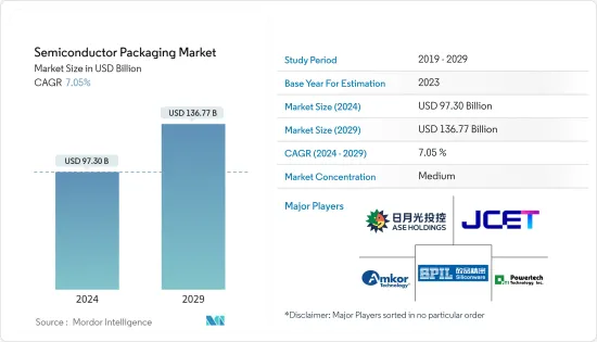
The Semiconductor Packaging Market size is estimated at USD 97.30 billion in 2024, and is expected to reach USD 136.77 billion by 2029, growing at a CAGR of 7.05% during the forecast period (2024-2029).
Semiconductor packaging refers to a casing that contains one or more discrete semiconductor devices or integrated circuits made up of plastic, ceramic, metal, or glass casing. Packaging is crucial for protecting an electronic system from radio frequency noise emission, electrostatic discharge, mechanical damage, and cooling.
High-performance computing, data center networking, and autonomous vehicles are pushing the adoption rates for the market studied and accelerating its technological evolution. The trend is to have more enormous computing resources at the cloud, edge computing, and device levels. The advancements in the market studied are also possible due to the growth in high-end performance applications and artificial intelligence (AI) in the telecom and infrastructure industry.
As the front-end node becomes smaller, design cost becomes increasingly important. Advanced packaging (AP) solutions aid in solving these problems by reducing the cost while enhancing system performance and offering lower latency, increased bandwidth, and power efficiency.
The increasing digitization of the workplace, the emergence of remote working and remote operation trends, and the growing consumer preference for electronics have increased the demand for semiconductor devices capable of unlocking a wide range of new opportunities. As the growth of semiconductor devices continues to accelerate, advanced packaging technologies provide the size and processing power necessary for the digitized era.
Global governments are increasingly supporting the semiconductor industry by lowering barriers and ramping up production, research, and development subsidies. For instance, South Korea committed a staggering USD 456 billion in private investments to construct the world's largest chip center, underlining its ambitions for industry dominance.
In tandem with this, the South Korean government rolled out an extensive support initiative for its semiconductor industry, valued at KRW 26 trillion (approximately USD 19.1 billion). This program spans financial aid, infrastructure development, R&D, and targeted assistance for its SMEs. Just outside Seoul, South Korea is currently in the works of creating a "mega chip cluster," which is projected to become the largest semiconductor hub globally and a key driver in creating numerous new employment opportunities.
A significantly high initial investment is required in designing, developing, and setting up semiconductor packaging units as per the requirements of different industries such as automotive, consumer electronics, healthcare, IT and telecommunication, and aerospace and defense. This can restrict the growth of the semiconductor packaging market.
Moreover, the defense budgets of various countries are significantly influenced by major macroeconomic factors such as inflation, economic growth, government spending priorities, and global trade and geopolitical dynamics.
In March 2023, President Joe Biden proposed the largest peacetime US defense budget, totaling USD 886 billion. This budget notably included a 5.2% pay raise for troops and marked the highest-ever allocation for research and development. The backdrop of Russia's actions in Ukraine further underscored the need for increased spending on munitions.
As per the US Congressional Budget Office, the United States is set to witness a consistent rise in defense spending, with projections extending until 2033. In 2023, the United States spent USD 746 billion on defense, with forecasts indicating a climb to USD 1.1 trillion by 2033.
Semiconductor Packaging Market Trends
The Communication and Telecom Segment to be the Fastest Growing End User
- The evolution in networking and connectivity is quite visible. It has evolved from the basic exchange of voice and visual signals through wired infrastructure to the current state of exchanging multimedia and large volumes of data through wireless infrastructure.
- Semiconductors are pivotal in telecom infrastructure, handling tasks from capturing and encoding data to encryption, transmission, and, ultimately, user presentation. 5G technology heralds a significant leap in telecommunication networks and devices, offering notably faster speeds than its predecessors and, crucially, boasting remarkably low latency. This reduced latency is especially vital for applications like cloud gaming and VR content streaming. Thus, the increasing demand for semiconductors in the communication and telecom industry is expected to propel the growth of the semiconductor packaging market.
- Similarly, in February 2024, the US government allocated a substantial USD 42 million toward fostering wireless innovation within the nation. This funding was earmarked for a collaborative project involving US carriers, international counterparts, leading universities, and equipment suppliers. The initiative aimed to set up a testing, evaluation, and R&D center in the Dallas Technology Corridor, complemented by a satellite facility in Washington, DC. The primary focus of these facilities would be testing network performance, ensuring interoperability, enhancing security measures, and spearheading research into novel testing methodologies.
- Similarly, in April 2023, Ericsson expressed its intention to collaborate with the Canadian government and invest CAD 470 million (USD 345.44 million) over five years. This investment was directed toward researching and developing technologies such as 6G, 5G advanced, artificial intelligence, Cloud RAN, and core networks. The objective of this initiative was to foster the growth of the telecommunications industry in the region and support the development of research facilities. These investments were poised to surge the demand for semiconductor devices due to their widespread use in the telecommunications industry, further bolstering the market's growth.
- In 2024, the telecommunications industry across emerging nations showcased a mix of technological advancements and strategic market development. Incorporating innovative and advanced semiconductor solutions played a vital role in this shift, meeting the increasing needs for connectivity and speed and addressing crucial elements like security, sustainability, and customized user experience. With ongoing progress, the collaboration between telecom and semiconductor technologies is expected to significantly influence the global digital landscape.
- The growing adoption of cloud technology, increasing penetration of data centers, and rising popularity of 5G technology are further bolstering the growth of the semiconductor packaging market. The increasing expansion of the data center and cloud market worldwide is expected to fuel the demand for data storage, further propelling the market's growth. For instance, according to Cloudscene, as of March 2024, there were 5,381 data centers in the United States, the most of any country worldwide.
Taiwan is Expected to Hold Significant Market Share
- Taiwan is home to some of the largest semiconductor manufacturers, such as TSMC (Taiwan Semiconductor Manufacturing Company) and United Microelectronics Corporation (UMC). The robust presence of these companies creates a demand for advanced packaging solutions.
- For instance, in March 2024, TSMC, considering the surging demand for AI chips, launched a significant expansion across Northern, Central, and Southern Taiwan. This expansion encompasses the introduction of 2-nanometer fabs and cutting-edge packaging plants. TSMC had even hinted at the potential need to invest in eight to ten facilities to support the upcoming 1-nanometer technology in Taiwan.
- The rising demand for AI chips is fueling the necessity for advanced packaging technologies, such as CoWoS (Chip-on-Wafer-on-Substrate). To meet this escalating demand, TSMC is ramping up its advanced packaging facilities in Zhunan, located in the heart of Taiwan's Science Park. The company will kick off tool-in and production line integration this year. Additionally, construction for an advanced packaging facility in Chiayi is slated to begin this year.
- The growth of Taiwan's digital economy to meet customers' needs and support products such as high-performance computing (HPC), artificial intelligence (AI), and mobile applications has created an opportunity for the semiconductor packaging market in Taiwan as its use in combining semiconductor dies on top of each other for miniaturized and high-performance applications of semiconductor chips. GSMA's forecast predicts that by 2025, over 50% of global mobile internet connections will be powered by 5G technology in Taiwan.
- For instance, in May 2023, Taiwan Semiconductor Manufacturing Co. (TSMC), the contract chip manufacturer, announced its plans to construct seven new facilities in 2024 to enhance its global competitive edge. These facilities would include three wafer plants, two packaging factories in Taiwan, and two overseas wafer plants. This expansion was a strategic response to the worldwide appetite for high-performance computing devices and smartphones. Construction commenced on an advanced packaging factory in Central Taiwan in 2023.
- Additionally, a facility in Chiayi is set to kick off later this year, with plans to roll out Chip-on-Wafer-on-Substrate (CoWoS) and small outline integrated circuit (SoIC) technologies by 2026. In June 2024, Taiwan's semiconductor company, TSMC, grappled with a soaring demand for its advanced technology. Key players like Apple and NVIDIA have fully booked TSMC's production, with orders stretching into 2026.
- In response to this surge, TSMC is eyeing a 5% hike in its 3 nm prices, while its advanced packaging rates could see a steeper rise of 10% to 20% in the coming year. TSMC's 3 nm lineup comprises N3, N3E, and N3P, alongside newer additions N3X and N3A. While the original N3 technology undergoes enhancements, N3E, which commenced mass production in Q4 of the previous year, is designed for AI accelerators, premium smartphones, and data centers.
- Semiconductors are used in various ways as tools and equipment in the healthcare industry. The expanding use of ultrasound technology encourages the use of semiconductor packaging in the country, which is in line with the growth of healthcare digitalization and electronic device usage in the country's hospitals. In Taiwan, manufacturers significantly focus on producing and exporting mid-to-low-end medical equipment through contract manufacturing for multinational companies.
- In January 2024, the International Trade Administration highlighted a surge in the country's medical device production by data from the Taiwan Ministry of Economic Affairs. The ministry published that the total local production in 2023 reached USD 8,928,333, marking a consistent upward trend and showing a promising growth trajectory for the market.
Semiconductor Packaging Industry Overview
The semiconductor packaging market is semi-consolidated with the presence of significant players like ASE Technology Holding Co. Ltd, Amkor Technology, Jiangsu Changjiang, Electronics Technology Co. Ltd (JCET), Siliconware Precision Industries Co. Ltd, and Powertech Technology Inc. Players in the market are adopting strategies, such as partnerships and acquisitions, to enhance their product offerings and gain sustainable competitive advantage.
- In April 2024, Samsung's AVP team received an order for advanced packaging for NVIDIA's AI chip, allowing for the future supply of high-bandwidth memory chips. The AVP team at Samsung Electronics will be responsible for providing interposer and 2.5D packaging technology for packaging NVIDIA's AI processors. However, the HBM and GPU chips used in these processors will come from other suppliers. The 2.5D packaging technology allows for the horizontal integration of chips such as CPUs, GPUs, and HBMs on an interposer.
- In December 2023, JCET opened the Semiconductor Packaging and Test Museum in Jiangyin, Jiangsu Province. The museum is a dedicated establishment that exhibits the realm of integrated circuit packaging and testing. It signifies a fresh endeavor by JCET to propel the packaging and testing industry. The museum acts as a prominent symbol for fostering science and technology in the IC sector within Jiangyin while also serving as a platform to showcase the accomplishments of the packaging and testing industry.
Additional Benefits:
- The market estimate (ME) sheet in Excel format
- 3 months of analyst support
TABLE OF CONTENTS
1 INTRODUCTION
- 1.1 Study Assumptions and Market Definition
- 1.2 Scope of the Study
2 RESEARCH METHODOLOGY
3 EXECUTIVE SUMMARY
4 MARKET INSIGHTS
- 4.1 Market Overview
- 4.2 Industry Attractiveness - Porter's Five Forces Analysis
- 4.2.1 Bargaining Power of Suppliers
- 4.2.2 Bargaining Power of Buyers
- 4.2.3 Threat of New Entrants
- 4.2.4 Threat of Substitutes
- 4.2.5 Intensity of Competitive Rivalry
- 4.3 Industry Value Chain Analysis
- 4.4 Impact of COVID-19 Aftereffects and Other Macroeconomic Factors on the Market
5 MARKET DYNAMICS
- 5.1 Market Drivers
- 5.1.1 Growing Consumption of Semiconductor Devices Across Industries
- 5.1.2 Favorable Government Policies and Regulations in Developing Countries
- 5.2 Market Restraints
- 5.2.1 High Initial Investment and Increasing Complexity of Semiconductor IC Designs
6 MARKET SEGMENTATION
- 6.1 By Packaging Platform
- 6.1.1 Advanced Packaging
- 6.1.1.1 Flip Chip
- 6.1.1.2 SIP
- 6.1.1.3 2.5D/3D
- 6.1.1.4 Embedded Die
- 6.1.1.5 Fan-in Wafer Level Packaging (FI-WLP)
- 6.1.1.6 Fan-out Wafer Level Packaging (FO-WLP)
- 6.1.2 Traditional Packaging
- 6.1.1 Advanced Packaging
- 6.2 By End-user Industry
- 6.2.1 Consumer Electronics
- 6.2.2 Aerospace and Defense
- 6.2.3 Medical Devices
- 6.2.4 Communications and Telecom
- 6.2.5 Automotive Industry
- 6.2.6 Energy and Lighting
- 6.3 By Geography
- 6.3.1 United States
- 6.3.2 China
- 6.3.3 Taiwan
- 6.3.4 South Korea
- 6.3.5 Japan
- 6.3.6 Europe
- 6.3.7 Latin America
- 6.3.8 Middle East and Africa
7 COMPETITIVE LANDSCAPE
- 7.1 Company Profiles
- 7.1.1 ASE Technology Holding Co. Ltd
- 7.1.2 Amkor Technology
- 7.1.3 Jiangsu Changjiang Electronics Technology Co. Ltd (JCET)
- 7.1.4 Siliconware Precision Industries Co. Ltd
- 7.1.5 Powertech Technology Inc.
- 7.1.6 Tianshui Huatian Technology Co. Ltd
- 7.1.7 Fujitsu Semiconductor Ltd
- 7.1.8 UTAC Holdings Ltd
- 7.1.9 Chipmos Technologies Inc.
- 7.1.10 Chipbond Technology Corporation
- 7.1.11 Intel Corporation
- 7.1.12 Samsung Electronics Co. Ltd
- 7.1.13 Unisem (M) Berhad
- 7.1.14 Interconnect Systems Inc. (ISI)
8 INVESTMENT ANALYSIS
9 FUTURE OF THE MARKET

