
PUBLISHER: Mordor Intelligence | PRODUCT CODE: 1642009

PUBLISHER: Mordor Intelligence | PRODUCT CODE: 1642009
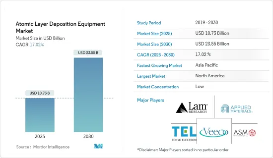
Atomic Layer Deposition Equipment - Market Share Analysis, Industry Trends & Statistics, Growth Forecasts (2025 - 2030)
The Atomic Layer Deposition Equipment Market size is estimated at USD 10.73 billion in 2025, and is expected to reach USD 23.55 billion by 2030, at a CAGR of 17.02% during the forecast period (2025-2030).
One of the key factors propelling the expansion of the worldwide atomic layer deposition market is the increasing adoption of electronics and semiconductor solutions across the globe.
Key Highlights
- Using novel materials and designs for improved chip production drives demand for atomic layer deposition solutions. The trend toward miniaturization is being embraced by industries all around the world. As a result, there is currently a higher need for tiny electronics and machinery.
- According to Cisco, around 500 billion devices will be connected to the Internet by 2030. Each machine includes sensors that collect data, interact with the environment, and communicate over a network. These applications need miniaturized storage devices and ICs. The increasing amount of data generated from the growing number of connected devices has increased the demand for storage devices, thereby driving market growth.
- High-k dielectric films used in CMOS processors, memory devices, MEMS, and sensors are frequently produced using ALD in the semiconductor industry. For the creation of functional and protective coatings in fuel cells and other applications needing corrosion or wear resistance, ALD technologies are used. For the development of next-generation devices, they are also utilized to coat high aspect ratio structures like nanowires and nanotubes.
- Due to the development of a large number of innovation and energy efficient technologies, demand for lightweight portable devices has increased rapidly. For the production of silicon chips, atomic layer deposition technology is widely used. In the end, the growth of the atomic layer deposition market is expected to be driven by increasing demand for electronic devices.
- Additionally, it is anticipated that greater robot use and manufacturing automation will promote the market for ALD technology by increasing semiconductor sales. Industrial automation is currently transforming the nature of practically all significant production industries. The adoption of Industry 4.0 standards and the increasing use of collaborative robotics, AR/VR, and AI for data analysis are anticipated to benefit the ALD market.
- Moreover, the ALD thin layer may be utilized in microelectronics to shield neighboring components in nanoscale transistors electrically. ALD is particularly adept at creating accurate, nanoscale coatings on intricate, 3D surfaces; such as the deep, narrow trenches etched into silicon wafers used to make modern computer processors. This has inspired researchers worldwide to create novel thin film ALD materials for upcoming semiconductor device generations.
- Over the projected period, a high investment required for research and development is anticipated to restrain the growth of the worldwide atomic layer deposition market. ALD is recognized to have significant limitations due to its slow approach.
Atomic Layer Deposition Equipment Market Trends
Semiconductors and Electronics Industry to Drive the Market Growth
- The demand from the semiconductor and electronics industries is anticipated to be the primary driver of atomic layer deposition technology. While the semiconductor industry is expected to impact the technology's development directly, any electronics industry expansion will contribute to its advancement. Consequently, atomic layer deposition equipment is growing in demand.
- After the global fab capacity expansions that manufacturers announced as a result of the chip shortfall, Atomic Layer Deposition (ALD) players are prepared to take advantage of a new growth opportunity. Recently, 300mm ALD platforms have improved to satisfy the requirement of More-than-Moore (MtM) devices and applications for MEMS, sensors, power and RF devices, and photonics. Previously, 200mm ALD platforms were designed to fulfill the market's needs. Now that wafer production has increased in volume, it is anticipated that ALD solutions will expand and join the MtM devices market.
- ALD rose to prominence in the semiconductor industry due to its use for depositing high-permittivity oxide materials. For example, thermally grown SiO2 was swapped out for HfO2 formed by ALD as the gate dielectric material in conventional metal oxide semiconductor field effect transistors. The number of applications requiring the usage of ALD has significantly increased in recent years.
- The electronics sector has ups and downs in cycles. The short- to medium-term outlook for the electronic industry is positive. By 2024, there will be around 8.9 billion mobile subscriptions, 8.4 billion mobile broadband subscriptions, and 6.2 billion unique mobile users, predicts the Ericsson Mobility Report. This is anticipated to accelerate the development of ALD technology.
- During the projection period, growth in the sales of consumer electronics and microelectronics is anticipated to drive up demand for semiconductor ICs. The increased demand for semiconductor ICs will raise the manufacturing capabilities of semiconductor device producers, which might increase demand for the atomic layer deposition equipment market.
- Next-generation semiconductor device production necessitates the deposition of highly conformal (great than 95%) SiO2, SiNx, and SiC films on high aspect-ratio nanostructures at low temperatures (400 °C). Atomic layer deposition is replacing chemical vapor deposition in semiconductor manufacturing, allowing for the development of these Si-based dielectric films. ALD-deposited SiO2 films are already utilized in the production of semiconductor devices.
- The expansion of RF and power electronics further aids the advancement of ALD technology. Extreme environmental conditions can damage and corrode active components, leading to early failure. These conditions include high temperatures, oxygen, ultraviolet radiation, salinity, and moisture. The performance and dependability of these components can be significantly increased for the same reason, thanks to atomic layer deposition (ALD).
Asia Pacific Expected to Witness the Highest Growth Rate
- The Asia Pacific continues to be the most critical region for the proliferation of the electronics industry. The Asia Pacific has become a hub of OEMs in the electronics industry. Moreover, emerging economies like Vietnam have invested heavily in this industry, leading to healthy competition among various regional countries. Moreover, established hubs like Taiwan and China continue to invest heavily in R&D, enabling them to stay ahead of the curve in innovations that drive market growth.
- Atomic layer deposition is commonly utilized in solar cells and devices for conformal coatings. In light of this, the target market is anticipated to develop throughout the projected period due to the increase in demand for solar devices and the rise in the solar industry across various regional countries. Additionally, governments in the APAC region are constantly establishing various investments to increase their solar industry, which drives the demand for ADL solutions.
- The automobile is another significant sector that uses ALD units and Systems for its manufacturing. Automobile industries are another primary user of thin film, as it is used in practically every aspect of the industry. For example, the thin film can reduce the size and enhance the life of various parts. Thin coatings are used in the automotive sector to save money and the environment. This is done by reducing the weight of commonly used construction elements, enhancing their service life, and, as a result, improving the manufacturing quality of nanomaterials.
- Asia is the home of some of the biggest manufacturers of automobiles in the world, such as Honda, Toyota, Mitsubishi, Nissan, Hyundai, TATA Motors, Maruti, etc., with countries like China and India, Japan, and South Korea being the powerhouse of Asian Automobile Sector. Apart from these OEMs, many parts and automobile accessories suppliers also find usage for ALD units and equipment for their manufacturing requirements.
- A critical approach in producing semiconductor devices is atomic layer deposition, a thin-film deposition process that relies on the use of a gas-phase chemical process. The market's players in this region are heavily investing in research and development programs to improve their outcomes' efficiency and lead the fastest market expansion worldwide.
Atomic Layer Deposition Equipment Industry Overview
The Atomic Layer Deposition Equipment Market is fragmented, as several players are operating in the market. Players in the market adopt strategies like mergers, acquisitions, and partnerships to capture market share.
- November 2023 - Oxford Instruments Plasma Technology announces significant order placements for plasma atomic layer deposition (ALD) and atomic layer etch (ALE) for GaN HEMT device production from several market-leading Japanese foundries. The systems will support high-growth GaN power electronics and radio frequency markets, with consumer fast-charging and datacentre applications at the forefront for power electronics, and 5G/6G communication applications for the radio frequency market.
- September 2023 - Sky water technology announced it will provide customers a new semiconductor processing tool for Applied Picosun MorpherTM, atomic layer deposition (ALD) . The thin layers that can be deposited uniformly across the entire silicon wafer are required by a number of devices, such as sensors and emerging memory technology.
Additional Benefits:
- The market estimate (ME) sheet in Excel format
- 3 months of analyst support
TABLE OF CONTENTS
1 INTRODUCTION
- 1.1 Study Assumptions and Market Definition
- 1.2 Scope of the Study
2 RESEARCH METHODOLOGY
3 EXECUTIVE SUMMARY
4 MARKET INSIGHTS
- 4.1 Market Overview
- 4.2 Industry Attractiveness - Porter Five Forces
- 4.2.1 Bargaining Power of Suppliers
- 4.2.2 Bargaining Power of Consumers
- 4.2.3 Threat of New Entrants
- 4.2.4 Threat of Substitute
- 4.2.5 Intensity of Competitive Rivalry
- 4.3 Industry Value Chain Analysis
- 4.4 Technology Snapshot : Comparison with other deposition technologies and evolution of ALD from Applications in Memory to Application in Logic MPUs and Qualitative analysis regarding type of ALD technologies
- 4.5 Assessment of COVID-19 Impact on the Industry
5 MARKET DYNAMICS
- 5.1 Market Drivers
- 5.1.1 Increase in demand of Microelectronics and Consumer Electronics
- 5.1.2 Advancement in Computing and Storage Technologies
- 5.2 Market Challenegs
- 5.2.1 Higher Associated costs due to Effective Deposition Reactants and Materials
6 MARKET SEGMENTATION
- 6.1 By Application
- 6.1.1 Semiconductor and Electronics (includes Computing Sector, Data Centres, and Consumer Electronics)
- 6.1.2 Healthcare and Biomedical Applications
- 6.1.3 Automotive
- 6.1.4 Other Applications
- 6.2 By Geography
- 6.2.1 Americas
- 6.2.2 Europe, Middle East and Africa
- 6.2.3 Asia
- 6.2.4 Australia and New Zealand
7 COMPETITIVE LANDSCAPE
- 7.1 Company Profiles
- 7.1.1 Applied Materials Inc.
- 7.1.2 Lam Research Corporation
- 7.1.3 Entegris Inc.
- 7.1.4 Veeco Instruments Inc.
- 7.1.5 Oxford Instruments PLC
- 7.1.6 Beneq Oy
- 7.1.7 Picosun Oy
- 7.1.8 ASM International
- 7.1.9 Tokyo Electron Limited
- 7.1.10 Kurt J. Lesker Company
8 INVESTMENT ANALYSIS
9 MARKET OPPORTUNITIES AND FUTURE TRENDS

