
PUBLISHER: Mordor Intelligence | PRODUCT CODE: 1550010

PUBLISHER: Mordor Intelligence | PRODUCT CODE: 1550010
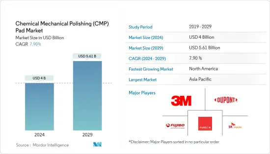
Chemical Mechanical Polishing (CMP) Pad - Market Share Analysis, Industry Trends & Statistics, Growth Forecasts (2024 - 2029)
The Chemical Mechanical Polishing Pad Market size is estimated at USD 4 billion in 2024, and is expected to reach USD 5.61 billion by 2029, growing at a CAGR of 7.90% during the forecast period (2024-2029).
Key Highlights
- Chemical mechanical polishing is a crucial step in the semiconductor wafer manufacturing process. During this process, the top surface of the wafer is polished to create a completely flat surface, which is essential for building more robust and durable semiconductor materials using a combination of chemical slurry and mechanical movements.
- The rising performance standards of electronic devices are leading to a need for smaller and more durable semiconductors and electronic devices. This, in turn, increases the requirement for advanced fabrication materials and techniques such as CMP. The growing demand for electronic products drives the electronic packaging industry, with customers expecting enhanced features in new electronic devices.
- The semiconductor industry is a significant consumer of chemical mechanical polishing pads, particularly for wafer polishing processes during semiconductor manufacturing. The increasing demand for semiconductors driven by applications such as automotive electronics, smartphones, IoT devices, and AI (artificial intelligence) technologies fuels the demand for chemical mechanical polishing pads. Moreover, the continuous technological advancements in semiconductor fabrication technologies, including the development of smaller feature sizes, drive the need for more precise and efficient CMP pads.
- The rising adoption of packaging technologies such as 3DE ICs, through-silicon vias(TSVs), and fan-out wafer-level packaging (FOWLP) necessitates advanced CMP polishing and surface preparation solutions. Chemical mechanical polishing (CMP) pads are crucial in achieving the required polishing, surface roughness, and defectivity levels of these advanced packaging processes.
- Despite the advancements in chemical mechanical polishing (CMP) pad materials and manufacturing processes, certain technological limitations persist. These limitations include achieving ultra-smooth surfaces, controlling sub-surface damage, minimizing edge effects, and addressing pad wear and slurry consumption issues. Overcoming these limitations may require further research and development efforts, thus hindering the market's growth. Moreover, CMP pad manufacturers may face risks associated with supply chain disruptions, impacting the ability to meet demand.
- Macroeconomic factors such as technological advancements, material science innovations, and process engineering developments are presenting challenges and opportunities for CMP pad manufacturers. Addressing technical difficulties related to CMP process control, defect reduction, material compatibility, and surface quality improvement drives R&D investments and product innovation in the CMP pads market. Conversely, breakthroughs in CMP pad materials, formulations, or manufacturing techniques can create competitive advantages and market opportunities for innovative suppliers.
Chemical Mechanical Polishing (CMP) Pad Market Trends
300 mm Wafer Size to Witness a Significant Growth
- The semiconductor industry has largely standardized around 300 mm wafer size for advanced manufacturing processes. This standardization simplifies supply chain logistics and facilitates collaboration among semiconductor manufacturers, equipment suppliers, and materials providers. As a result, chemical mechanical polishing (CMP) pad manufacturers prioritize developing and producing CMP pads designed for 300 mm wafer processing to meet the industry demand.
- The rate of global 300 mm fab capacity expansion is slowing down. However, the industry is still dedicated to increasing capacity to keep up with the firm and consistent semiconductor demand. For instance, in March 2024, India planned to produce equipment for semiconductor manufacturing, with Applied Materials taking the lead by establishing a validation center in Bengaluru. The country is also advancing in 300 mm wafer processing and is focusing on creating a supportive ecosystem while establishing an engineering center. These innovations are driving the growth of the market studied.
- In November 2023, Texas Instruments launched a new 300 mm semiconductor wafer fabrication plant called LFAB2 in Lehi, Utah. The construction of LFAB2 will be connected to the company's existing 300 mm wafer fab in the exact location. Once LFAB2 is finished, both of TI's Utah fabs will be capable of producing tens of millions of embedded and analog processing chips daily at maximum capacity. LFAB2 aims to operate solely on renewable electricity, and the implementation of advanced 300 mm equipment and processes in Lehi will help minimize waste, water, and energy usage.
- The shift to 300 mm wafer size is often associated with adopting advanced semiconductor manufacturing technologies and smaller process nodes (7 nm and 5 nm). These advanced node technologies require tighter process control and enhanced polishing to meet stringent performance and reliability requirements.
- Chemical mechanical polishing (CMP) pads are in high demand because they play a crucial role in achieving the nanoscale-level planarity required for advanced node fabrication.
Asia-Pacific to Hold Significant Market Share
- Asia-Pacific is a global semiconductor manufacturing hub, with countries like China, Taiwan, South Korea, and Japan playing significant roles in semiconductor fabrication. The region's growth in semiconductor manufacturing drives the substantial demand for chemical mechanical polishing (CMP) pads used in wafer polishing processes.
- Asia-Pacific is at the forefront of technological advancements, including developing advanced packaging technologies, high-performance computing, and AI (artificial intelligence). These advancements require precise and efficient CMP processes, boosting the demand for CMP pads.
- The region continues to witness investments in new semiconductor fabrication facilities (fabs) and the expansion of existing ones. Increasing fab capacity and installing advanced manufacturing equipment contribute to the higher consumption of CMP pads. For instance, in March 2024, Tata Electronics Private Limited (TEPL) partnered with Taiwan's Powerchip Semiconductor Manufacturing Corp. (PSMC) to set up a semiconductor fab in Dholera, Gujarat. The investment for this project is INR 9,100 billion (USD 109.71 billion). PSMC currently operates six semiconductor foundries in Taiwan.
- The capacity of the new fabs will be 50,000 wafer starts per month. PSMC will focus on producing high-performance compute chips using 28 nm technology and power management chips for various industries such as electric vehicles, telecom, defense, automotive, consumer electronics, display, and power electronics.
- Asia-Pacific is home to a large and expanding consumer electronics market driven by rising disposable incomes, urbanization, and technological proliferation. The demand for smartphones, laptops, and electronic devices fuels the need for semiconductor components and CMP pads.
- Moreover, emerging economies in Asia-Pacific, such as India, Vietnam, and Indonesia, are witnessing increasing adoption of semiconductor technologies across various sectors. As these economies continue to industrialize and digitize, the demand for CMP pads for semiconductor manufacturing is expected to grow significantly.
- Ongoing infrastructure development projects, such as smart cities, 5G networks, and the IoT, drive demand for semiconductor chips and electronic components. The chemical mechanical polishing (CMP) pads play a significant role in enabling the production of advanced semiconductor devices required for these infrastructure projects.
- In addition, governments and industries in Asia-Pacific are investing in semiconductor R&D to foster innovation. Research initiatives aimed at developing next-generation materials, devices, and processes contribute to the demand for CMP pads.
Chemical Mechanical Polishing (CMP) Pad Industry Overview
The chemical mechanical polishing (CMP) pads market is very competitive. It is highly concentrated due to various large and small players. All the major players account for a significant market share and focus on expanding the global consumer base. Some significant players in the market are 3M Co, DuPont de Nemours Inc., Fujibo Holdings Inc., Pureon, and SK enpulse. Several companies are increasing their market share by forming collaborations, partnerships, and acquisitions and introducing new and innovative products to earn a competitive edge during the forecast period.
- In April 2024, SK Hynix was set to continue with its scheduled investments in Korea. The company is getting the Yongin Semiconductor Cluster site ready to construct production facilities, with an investment of JPY 120 trillion (USD 0.74 trillion). The first fab was expected to start construction in March 2025 and be completed by early 2027. A mini fab will also be constructed to test semiconductor materials, components, and equipment using 300 mm wafer processing equipment.
- In September 2023, SK enpulse divested its semiconductor basic materials business, with the wet chemical business purchased by the local semiconductor/display materials company Yaker Technology and the cleaning business acquired by the investment company Sunyang Shinjin. Earlier this year, SKC consolidated its semiconductor materials/parts businesses into SK enpulse to enhance its presence in high-value-added materials business areas for semiconductor front-end processes, such as chemical mechanical polishing (CMP) pads and blank masks.
Additional Benefits:
- The market estimate (ME) sheet in Excel format
- 3 months of analyst support
TABLE OF CONTENTS
1 INTRODUCTION
- 1.1 Study Assumptions and Market Definition
- 1.2 Scope of the Study
2 RESEARCH METHODOLOGY
3 EXECUTIVE SUMMARY
4 MARKET INSIGHTS
- 4.1 Market Overview
- 4.2 Industry Attractiveness - Porter's Five Forces Analysis
- 4.2.1 Threat of New Entrants
- 4.2.2 Bargaining Power of Buyers/Consumers
- 4.2.3 Bargaining Power of Suppliers
- 4.2.4 Threat of Substitute Products
- 4.2.5 Intensity of Competitive Rivalry
- 4.3 Technology Snapshot
- 4.4 Impact of COVID-19 Aftereffects and Other Macroeconomic Factors on the Market
5 MARKET DYNAMICS
- 5.1 Market Drivers
- 5.1.1 Increasing Need for Complex and High-Performance Chips/Advanced Technologies
- 5.1.2 Introduction of Smaller Nodes and New Architectures
- 5.2 Market Restraints
- 5.2.1 Cyclic and Dynamic Nature of the Semiconductor Industry
6 MARKET SEGMENTATION
- 6.1 By Wafer Size
- 6.1.1 300 mm
- 6.1.2 200 mm
- 6.1.3 Other Wafer Sizes
- 6.2 By Geography
- 6.2.1 North America
- 6.2.2 Europe
- 6.2.3 China
- 6.2.4 South Korea
- 6.2.5 Japan
- 6.2.6 Taiwan
7 COMPETITIVE LANDSCAPE
- 7.1 Company Profiles
- 7.1.1 3M Co.
- 7.1.2 DuPont de Nemours Inc.
- 7.1.3 Fujibo Holdings Inc.
- 7.1.4 Pureon
- 7.1.5 SK enpulse
- 7.1.6 Thomas West Inc.
- 7.1.7 Hubei DingLong
- 7.1.8 Cabot Corporation
- 7.1.9 Entegris
- 7.1.10 Beijing Grish Hitech Co. Ltd
8 INVESTMENT ANALYSIS
9 FUTURE OF THE MARKET

