
PUBLISHER: Global Market Insights Inc. | PRODUCT CODE: 1699355

PUBLISHER: Global Market Insights Inc. | PRODUCT CODE: 1699355
Lithography Equipment Market Opportunity, Growth Drivers, Industry Trend Analysis, and Forecast 2025-2034
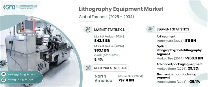
The Global Lithography Equipment Market was valued at USD 42.8 billion in 2024 and is projected to grow at a CAGR of 8.4% from 2025 to 2034. This growth is fueled by the surging demand for advanced and compact semiconductor components, particularly in consumer electronics. As modern electronic devices continue to evolve, manufacturers are pushing the boundaries of semiconductor design to enhance processing power, energy efficiency, and overall performance. This growing complexity is driving the adoption of cutting-edge lithography technologies, ensuring the production of high-density chips with superior functionality.
The semiconductor industry is experiencing rapid advancements in chip manufacturing processes, with lithography equipment playing a crucial role in enabling next-generation devices. The increasing integration of artificial intelligence, the Internet of Things (IoT), and 5G technology is further amplifying the need for high-performance chips, creating a strong demand for advanced lithography solutions. Moreover, the competitive nature of the semiconductor industry has led to continuous innovation in lithography techniques, allowing manufacturers to achieve higher precision and efficiency in semiconductor fabrication. As the semiconductor industry moves toward more intricate architectures, the reliance on lithography equipment continues to expand, making it a key driver of technological progress.
| Market Scope | |
|---|---|
| Start Year | 2024 |
| Forecast Year | 2025-2034 |
| Start Value | $42.8 Billion |
| Forecast Value | $93.1 Billion |
| CAGR | 8.4% |
The market is segmented by technology into ArF, KrF, i-line, ArF immersion, and Extreme Ultraviolet (EUV) Lithography. Among these, the ArF segment was valued at USD 11 billion in 2024 and is set for significant growth, particularly due to its applications in fast-growing industries like video streaming, online gaming, and virtual and augmented reality. ArF technology delivers enhanced performance within Deep Ultraviolet (DUV) lithography, which is essential for producing high-performance, high-density semiconductor devices. As the need for powerful and efficient chips increases, the ArF segment is expected to expand further, reinforcing its role in driving semiconductor innovation.
Lithography equipment is further categorized by type, including optical lithography, electron beam lithography, mask aligners, ion lithography, X-ray lithography, and nanoimprint lithography. Among these, optical lithography, also known as photolithography, remains the dominant segment and is projected to reach USD 63.3 billion by 2034. Its widespread adoption is attributed to its seamless integration into existing semiconductor production facilities, making it a cost-effective and scalable solution for chipmakers. With continuous advancements improving resolution and efficiency, optical lithography remains a preferred choice for semiconductor manufacturing, ensuring its strong market presence in the years ahead.
North America lithography equipment market is set for substantial growth, projected to reach USD 7.4 billion by 2034. This surge is driven by rising semiconductor demand across industries such as automotive, consumer electronics, and data centers. Efforts to strengthen supply chain resilience and bring semiconductor manufacturing back to domestic regions are further fueling market expansion. Additionally, North America's emphasis on research and development, coupled with a highly skilled workforce, is accelerating innovation in lithography technology, positioning the region as a key hub for semiconductor advancements.
Table of Contents
Chapter 1 Methodology and Scope
- 1.1 Market scope and definitions
- 1.2 Research design
- 1.2.1 Research approach
- 1.2.2 Data collection methods
- 1.3 Base estimates and calculations
- 1.3.1 Base year calculation
- 1.3.2 Key trends for market estimation
- 1.4 Forecast model
- 1.5 Primary research and validation
- 1.5.1 Primary sources
- 1.5.2 Data mining sources
Chapter 2 Executive Summary
- 2.1 Industry 360° synopsis
Chapter 3 Industry Insights
- 3.1 Industry ecosystem analysis
- 3.2 Industry impact forces
- 3.2.1 Growth drivers
- 3.2.1.1 Rising demand for advanced and miniaturized semiconductor components in consumer electronics
- 3.2.1.2 Technological advancements in the lithography process
- 3.2.1.3 Increasing demand for electrification in vehicles and the global proliferation of electric vehicles
- 3.2.1.4 Increasing trend toward IoT and AI technology around the globe
- 3.2.1.5 Growing demand for Compact and Power-Efficient Devices
- 3.2.2 Industry pitfalls and challenges
- 3.2.2.1 High production cost
- 3.2.2.2 Security concerns
- 3.2.1 Growth drivers
- 3.3 Growth potential analysis
- 3.4 Regulatory landscape
- 3.5 Technology landscape
- 3.6 Future market trends
- 3.7 Gap analysis
- 3.8 Porter's analysis
- 3.9 PESTEL analysis
Chapter 4 Competitive Landscape, 2024
- 4.1 Introduction
- 4.2 Company market share analysis
- 4.3 Competitive analysis of major market players
- 4.4 Competitive positioning matrix
- 4.5 Strategy dashboard
Chapter 5 Market Estimates and Forecast, By Technology, 2021 – 2034 (USD Mn)
- 5.1 Key trends
- 5.2 ArF
- 5.3 KrF
- 5.4 i-line
- 5.5 Arf immersion
- 5.6 Extreme Ultraviolet (EUV) Lithography
Chapter 6 Market Estimates and Forecast, By Equipment, 2021 – 2034 (USD Mn)
- 6.1 Key trends
- 6.2 Optical Lithography/Photolithography
- 6.3 Mask aligners
- 6.4 Electron beam lithography
- 6.5 Ion lithography
- 6.6 X-Ray lithography
- 6.7 Nanoimprint lithography
Chapter 7 Market Estimates and Forecast, By Application, 2021 – 2034 (USD Mn)
- 7.1 Key trends
- 7.2 Advanced packaging
- 7.3 MEMS devices
- 7.4 LED devices
- 7.5 Others
Chapter 8 Market Estimates and Forecast, By End Use, 2021 – 2034 (USD Mn)
- 8.1 Key trends
- 8.2 Electronics manufacturing
- 8.3 Healthcare and Life sciences
- 8.4 Automotive industry
- 8.5 Telecommunications
- 8.6 Others
Chapter 9 Market Estimates and Forecast, By Region, 2021 – 2034 (USD Mn)
- 9.1 Key trends
- 9.2 North America
- 9.2.1 U.S.
- 9.2.2 Canada
- 9.3 Europe
- 9.3.1 UK
- 9.3.2 Germany
- 9.3.3 France
- 9.3.4 Italy
- 9.3.5 Spain
- 9.4 Asia Pacific
- 9.4.1 China
- 9.4.2 Japan
- 9.4.3 India
- 9.4.4 South Korea
- 9.4.5 ANZ
- 9.4.6 Taiwan
- 9.5 Latin America
- 9.5.1 Brazil
- 9.5.2 Mexico
- 9.6 Middle East and Africa
- 9.6.1 Saudi Arabia
- 9.6.2 UAE
- 9.6.3 Israel
- 9.6.4 South Africa
Chapter 10 Company Profiles
- 10.1 ASML Holding N.V.
- 10.2 Nikon Corporation
- 10.3 Canon Inc.
- 10.4 Veeco Instruments Inc.
- 10.5 SUSS MicroTec AG
- 10.6 EV Group
- 10.7 SCREEN Holdings Co., Ltd.
- 10.8 Onto Innovation Inc.
- 10.9 JEOL Ltd
- 10.10 Neutronix Quintel Inc. (NXQ)
- 10.11 Advantest
- 10.12 Shanghai Micro Electronics Equipment (Group) Co., Ltd.

